Synopsis
The entire digital world, from smartphones to supercomputers, hinges on the capacity to shrink electronic components, a feat achieved primarily through photolithography. This process of etching intricate patterns onto silicon wafers is executed by a device known as the semiconductor lithography machine, often regarded as the most complex piece of equipment ever built. This blog provides a foundational look into the technology that underpins the microchip industry, focusing on the specialized ecosystem of semiconductor lithography equipment manufacturers. We will delve into the core components that drive resolution and throughput, exploring the precision optics and mechanics that make up the intricate lithography machine components. Understanding the global landscape of lithography machine companies is vital, as a select few dominate the market. Furthermore, for those looking to invest or enter the market, we shed light on the astronomical costs involved, discussing factors that influence the semiconductor lithography machine price and the general availability of a semiconductor lithography machine for sale. This critical technology ensures that the steady advancement of Moore’s Law continues, empowering the next generation of digital innovation.
Table of Contents
-
The Foundation of the Digital World
-
Inside the Semiconductor Lithography Machine
-
The Intricate Lithography Machine Components
-
Precision Micromachining for Critical Environments
-
The Global Landscape of Equipment Manufacturers
-
Evaluating Investment: Semiconductor Lithography Machine Price
-
Laser Beam Delivery Systems
-
Addressing the Supply Chain and Availability
-
The Future: Extreme Ultraviolet (EUV) Technology
-
Dynotech’s Link to High-Precision Photonics
-
Supporting India’s Microelectronics Ambition
The Foundation of the Digital World
The modern microchip, containing billions of transistors etched onto a piece of silicon smaller than a thumbnail, is a miracle of engineering made possible by one critical technology: lithography. This process is analogous to using a high-precision camera to photograph a microscopic circuit design onto a light-sensitive polymer (photoresist) layered on the silicon wafer. The resulting pattern then guides the etching and doping processes that build the transistor layers. The quality, resolution, and speed of this pattern transfer directly determine the chip’s performance and cost. The machine responsible for this demanding task, the semiconductor lithography machine, is the bottleneck and the most significant piece of capital expenditure in any chip fabrication plant, or “fab.”
Inside the Semiconductor Lithography Machine
At its core, a semiconductor lithography machine is an optical projection system that uses deep ultraviolet (DUV) or, more recently, extreme ultraviolet (EUV) light to print patterns finer than the wavelength of the light itself. Achieving this extreme resolution—currently down to the single-digit nanometer scale—requires environmental control that is nearly perfect, including vibration isolation, precise temperature management, and vacuum operation for EUV systems. The machine must align the mask (reticle) with the wafer with picometer accuracy while exposing the pattern across the entire wafer surface in a step-and-scan or step-and-repeat motion, all within a fraction of a second. This continuous, high-speed, and ultra-precise action is what separates the capabilities of leading semiconductor lithography equipment manufacturers from standard optical component suppliers.
The Intricate Lithography Machine Components
The complexity of the system is best understood by examining the high-precision lithography machine components that work in concert to deliver the pattern. These include ultra-stable light sources (lasers), the reticle (mask) stage that holds the pattern, the projection optics (which can include dozens of complex, near-perfect lenses or mirrors), and the highly sophisticated wafer stage that moves the silicon during exposure. Each of these components must operate with fidelity measured in nanometers, requiring incredibly precise motion controls and sensors. The cleanliness standards are equally strict, often involving advanced vacuum systems and controlled purging to prevent airborne particles from ruining the microscopic patterns being drawn.
Precision Micromachining for Critical Environments
Dynotech’s expertise in laser micromachining, in collaboration with partners like OpTek Systems, directly addresses the demands of the semiconductor and photonics industries. We specialize in non-conventional materials and extreme precision, capable of fabricating microfiltration systems, glass components, and sensitive sensor parts. This capability to achieve micron precision through finely controlled laser material removal is vital for producing the highly specialized components, optics, and tooling used within the ultra-clean and critical environments of the semiconductor lithography equipment manufacturers.
The Global Landscape of Equipment Manufacturers
The global market for advanced semiconductor lithography equipment manufacturers is one of the most concentrated and strategically important sectors in the world. A small number of specialized lithography machine companies, primarily in Europe and Asia, dominate the fabrication industry, with one company notably holding a near-monopoly on the most advanced EUV technology required for producing the latest generation of microchips. These manufacturers operate at the very edge of physics and engineering, investing billions in research and development to push the boundaries of resolution and throughput. Their technological roadmaps effectively dictate the timeline for the advancement of consumer electronics, artificial intelligence, and high-performance computing capabilities worldwide.
Evaluating Investment: Semiconductor Lithography Machine Price
Given the intense research, development, and strategic nature of this equipment, the investment required is monumental, directly affecting the semiconductor lithography machine price. The price tag for a leading-edge EUV machine can easily exceed hundreds of millions of US dollars, making it the single most expensive piece of industrial machinery globally. Even older generation DUV systems represent a multi-million dollar investment. This high barrier to entry significantly limits the number of companies and nations that can participate in cutting-edge chip manufacturing. Furthermore, due to the high demand and limited production capacity of semiconductor lithography equipment manufacturers, the lead times for new machines can often stretch for years.
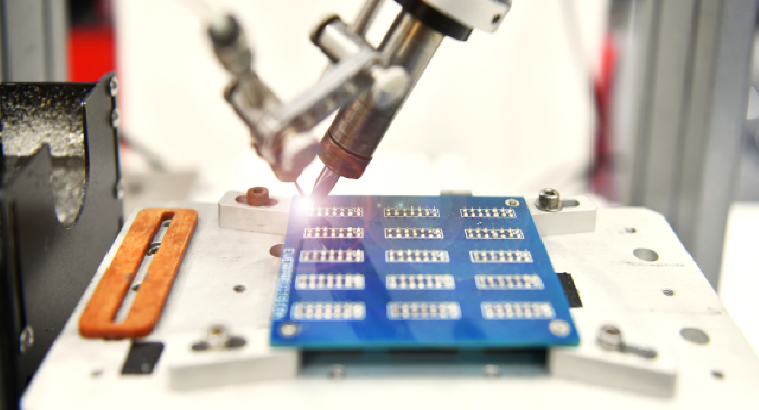
Laser Beam Delivery Systems
The performance of any high-power laser system, including those used for advanced lithography and subsequent wafer processing (such as trimming or dicing), relies heavily on robust beam management. Dynotech supplies custom-built, high-precision laser beam delivery systems, featuring modular components for all standard wavelengths. These systems—comprising mirrors, shutters, collimators, and focusing heads—are crucial for safely and accurately transporting the intense laser beam from the source to the wafer surface. Our solutions ensure minimal energy loss and maintain beam quality, a non-negotiable requirement for high-fidelity patterning in high-end semiconductor manufacturing environments.
Addressing the Supply Chain and Availability
For manufacturers and new market entrants, navigating the availability of machinery, or a semiconductor lithography machine for sale, presents considerable challenges. The primary market is dominated by the strategic allocation of new machines to the largest chip fabrication companies. Secondary markets for older generation DUV machines exist but are constrained by geopolitical factors and the difficulty of acquiring specialized support and maintenance outside the official channels of the lithography machine companies. For countries like India aiming to establish a domestic chip manufacturing ecosystem, securing these crucial machines, even older models, requires significant government and industrial coordination to ensure a stable supply pipeline and access to essential technical support infrastructure.
The Future: Extreme Ultraviolet (EUV) Technology
The future of lithography is already defined by the transition to Extreme Ultraviolet (EUV) technology, which uses a 13.5 nm wavelength to achieve the smallest possible feature sizes on a chip. This technology requires a complete vacuum environment and complex mirror optics instead of lenses, representing the pinnacle of precision engineering. Looking further ahead, researchers are exploring techniques such as high-NA (numerical aperture) EUV and directed self-assembly, which will continue the industry’s march towards ever smaller and more powerful transistors. This continuous evolution means that the demands placed on semiconductor lithography equipment manufacturers for resolution and throughput will only intensify.
Dynotech’s Link to High-Precision Photonics
Dynotech Instruments Pvt. Ltd. actively supports the peripheral, yet vital, precision requirements of the microelectronics industry. While we may not supply the core semiconductor lithography machine itself, our expertise in high-precision laser components, advanced lithography machine components delivery systems, and laser micromachining directly contributes to the development and maintenance of equipment utilized in the chip manufacturing process.
Supporting India's Microelectronics Ambition
By providing best-in-class instrumentation and expertise from leading global partners, Dynotech ensures that local research facilities and peripheral manufacturing operations have access to the highest quality components necessary to engage with the complex demands of the microchip supply chain, supporting India’s long-term goal of fostering domestic electronic manufacturing capability.
FAQs
What is the primary function of a semiconductor lithography machine, and why is it so critical to chip manufacturing?
The primary function of a semiconductor lithography machine is to optically transfer a microscopic circuit pattern from a photomask onto a silicon wafer coated with a light-sensitive material called photoresist. It is the defining technology in chip manufacturing because it determines the minimum feature size, or resolution, that can be achieved on the chip. Since performance and transistor density are directly related to this size, the capabilities of the lithography equipment essentially dictate the speed, power efficiency, and cost of the final integrated circuit. Without this precision equipment, modern microprocessors and memory chips, which drive the entire digital economy, simply could not be produced.
Which are the main global semiconductor lithography equipment manufacturers and why is their market so concentrated?
The market is dominated by a very small number of semiconductor lithography equipment manufacturers, with one company holding a virtual monopoly on the most advanced EUV (Extreme Ultraviolet) systems. The market is concentrated because the technological barrier to entry is immense, requiring decades of research and development and billions of dollars in investment to master the complex physics and engineering involved. These lithography machine companies must perfect every aspect of the technology—from the light source to the optics and the motion control—to operate at the very edge of physical limits, a feat few companies can achieve or sustain financially.
What factors account for the extremely high semiconductor lithography machine price?
The exceptionally high semiconductor lithography machine price is driven by several factors, mainly the extraordinary precision and complexity of the technology. The development cost alone, particularly for EUV systems, runs into billions of dollars. The required lithography machine components, such as the near-perfect, distortion-free optics, the vibration-dampened stages, and the high-power, multi-million dollar laser sources, are custom-made and extremely expensive to produce. Furthermore, the specialized assembly and calibration required to ensure nanometer accuracy contribute significantly to the final cost, making the machinery the single largest capital expenditure in a chip fabrication plant.
What are the key lithography machine components that must work together to achieve nanometer-scale precision?
The core lithography machine components essential for nanometer-scale precision include the light source (e.g., DUV or EUV laser), the reticle (or mask) stage which holds the circuit pattern, and the projection optics system (comprising many highly polished lenses or mirrors). Crucially, the wafer stage, which moves the silicon wafer beneath the projected light, must operate with flawless speed and precision, typically corrected thousands of times per second by advanced feedback sensors. Any mechanical or thermal instability in any of these major components can cause misalignment or pattern errors, making their synchronization vital for reliable manufacturing.
Is it feasible for a new company or a developing nation to acquire a semiconductor lithography machine for sale on the secondary market?
While it is possible to find a used or older generation semiconductor lithography machine for sale on the secondary market, it presents significant challenges. Acquiring the machine is only the first step; the buyer must also secure a sustainable supply chain for maintenance, specialized spare parts, and, critically, technical support from the original lithography equipment manufacturers. Furthermore, the installation and operation of the machine require a highly controlled, ultra-clean environment and a specialized, expensive support infrastructure that many new entrants or developing regions struggle to establish, making the operational setup as challenging as the initial purchase.