
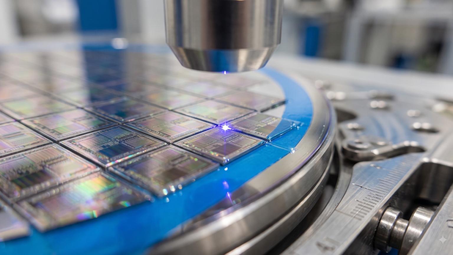
Synopsis
As semiconductor chips become smaller and more densely packed, legacy mechanical dicing saws and nanosecond thermal lasers cause unacceptable edge chipping, micro-cracking, and wafer degradation. To maximize silicon die yield per wafer, advanced semiconductor packaging facilities are adopting sub-picosecond cold machining tools that carve clean micro-grooves without thermal stress. Dynotech provides comprehensive sales facilitation and technical consulting for Clark-MXR micromachining systems throughout the Indian market.
We work closely with your process engineers from initial material testing and sample validation straight through to factory floor integration. To protect your capital investment from sudden production stoppages, Dynotech delivers localized laser maintenance, rapid spare parts delivery, and continuous technical support. Our certified field engineers perform optical realignments, clean enclosed beam paths, and calibrate motion stages to maintain sub-micron cutting accuracy. Upgrading your wafer processing lines with these advanced ultrafast platforms reduces scrap rates and drives long-term manufacturing efficiency.
Table of Contents
- Structural Limitations of Mechanical Saws and Thermal Lasers in Wafer Dicing
- Sub-Picosecond Mechanics and the Superiority of Cold Machining Tools
- Maximizing Die Yield per Wafer in Advanced Semiconductor Packaging
- Accelerated Procurement through End-to-End Sales Facilitation
- Safeguarding Cleanroom Throughput with Localized Laser Maintenance
- Minimizing Line Stoppages via Responsive Local Technical Support
- Advancing Indian Micro-Electronics Manufacturing with Dynotech Expertise
- Complete Clark-MXR Hardware Sales and Engineering Care Across India
Structural limitations of mechanical saws and thermal lasers in wafer dicing
The rapid evolution of semiconductor packaging toward ultra-thin silicon wafers, stacked die architectures, and delicate low-k dielectric materials has pushed legacy dicing technologies to their absolute physical limits. For decades, semiconductor back-end assembly facilities have relied on diamond blade mechanical saws or nanosecond thermal lasers to singulate individual silicon dies from full wafers. However, mechanical dicing saws apply severe physical vibration and shear stress to the wafer, leading to top-surface micro-chipping, backside delamination, and street width widening that wastes valuable silicon real estate. Similarly, nanosecond lasers rely on photothermal melting, which creates large thermal affected zones, silicon recast dross, and micro-cracks along the dicing street. These thermal and mechanical micro-defects weaken the mechanical strength of the individual die, increasing the risk of chip failure during wire bonding, encapsulation, or field operation. To increase die density per wafer and maintain high package reliability, modern semiconductor packaging plants must replace destructive mechanical and thermal cutting tools with non-contact, ultra-precise laser singulation solutions.
Sub-picosecond mechanics and the superiority of cold machining tools
To overcome the physical destruction caused by mechanical saws and thermal melting, advanced semiconductor packaging lines are transitioning to ultrafast sub-picosecond cold machining tools. Operating with pulse durations measured in picoseconds (10-12 seconds) or femtoseconds (10-15 seconds), these ultrafast laser systems deliver extremely high peak power densities that induce non-linear multiphoton absorption directly at the focal volume. Material bonds are broken instantly through direct ionization before thermal energy can transfer to the surrounding silicon crystal lattice. This unique energy delivery mechanism defines true cold machining tools, enabling clean material ablation with virtually zero heat affected zones, zero thermal stress, and zero recast dross. Because the material is vaporized cleanly at the atomic level, the dicing street width can be compressed down to sub-10 micron dimensions without causing edge chipping or dielectric layer peeling. Utilizing ultrafast cold machining tools allows semiconductor manufacturers to singulate delicate, ultra-thin wafers cleanly while maintaining exceptional mechanical die strength.
Maximizing die yield per wafer in advanced semiconductor packaging
The primary commercial benefit of deploying ultrafast laser cold machining tools in semiconductor wafer dicing is a significant increase in usable die yield per wafer. Because ultrafast lasers produce extremely narrow, burr-free dicing streets without micro-cracking, chip designers can shrink the kerf width spacing between adjacent dies on the silicon wafer map. Reducing the dicing street width allows semiconductor foundries to pack more active dies onto every single 200mm or 300mm silicon wafer, maximizing total yield per production run. Furthermore, eliminating physical vibration and thermal stress prevents edge chipping and micro-cracking, dramatically lowering the percentage of rejected dies during final electrical sorting and optical inspection. The combination of higher die density per wafer and reduced part scrap directly lowers manufacturing costs per die, giving semiconductor companies a strong competitive edge in the global market.
Accelerated procurement through end-to-end sales facilitation
Acquiring advanced ultrafast laser micromachining equipment for cleanroom installation requires a streamlined, highly reliable supply chain partner. International procurement of high-precision semiconductor processing machinery involves complex import regulations, dual-use technology compliance, air freight logistics, and strict cleanroom delivery protocols. Dynotech provides comprehensive, end-to-end sales facilitation for Clark-MXR ultrafast laser platforms across the Indian market, managing every phase of procurement directly. Our sales facilitation services cover initial hardware selection, cleanroom layout engineering, import documentation, customs clearance, and physical installation by certified field service engineers. Providing a transparent, hassle-free purchasing workflow allows Indian semiconductor facilities to acquire world-class micromachining technology quickly and efficiently without managing complex international logistics internally.
Safeguarding cleanroom throughput with localized laser maintenance
Maintaining sub-micron dicing precision and ultra-stable pulse energy in continuous 24/7 semiconductor manufacturing demands structured hardware care and dedicated localized laser maintenance. Ultrafast laser systems contain ultra-precise optical amplifiers, galvo scan heads, and motion stages that must operate within tight thermal and optical tolerances inside cleanroom environments. Dynotech delivers comprehensive localized laser maintenance programs tailored specifically to protect semiconductor back-end manufacturing operations. Our certified field service engineers conduct scheduled maintenance visits to clean enclosed beam delivery pathways, align pulse compressor optics, calibrate power output, inspect thermoelectric cooling loops, and replace aging pump diodes. Implementing proactive localized laser maintenance prevents sudden beam degradation, preserves micron-level kerf positioning, and extends the operational working life of your capital equipment investment.
Minimizing line stoppages via responsive local technical support
In high-volume semiconductor packaging facilities, an unexpected machine stoppage or laser driver fault can halt automated packaging lines, resulting in thousands of dollars in lost hourly output. Relying on overseas field service teams leads to frustrating equipment downtime while waiting for international travel arrangements and spare parts shipments. Dynotech eliminates this operational risk by delivering rapid, highly responsive local technical support across all major industrial and technology centers in India. Our certified service engineers carry specialized diagnostic tools, laser beam profilers, and maintain local inventories of critical spare parts, including optical modules, power supplies, and control boards. When a technical issue occurs, our team provides immediate remote diagnostics or deploys directly to your cleanroom facility to perform optical alignments, module repairs, and system recalibrations. Having reliable local technical support ensures your wafer processing lines stay fully operational, keeping your customer delivery schedules on track.
Advancing Indian micro-electronics manufacturing with Dynotech expertise
Building a robust, competitive semiconductor manufacturing ecosystem in India requires a trusted technology partner with deep process authority and multi-disciplinary experience. Dynotech stands as India’s premier high-technology integrator, bringing over 14 years of specialized expertise in lasers, semiconductors, precision machining, and production efficiency to every client partnership. We bridge the gap between global technology pioneers like Clark-MXR, Inc. and local cleanroom factory execution. Our comprehensive service model covers hardware sales facilitation, custom process consulting, cleanroom tool integration, operator training, and ongoing technical support. By working closely with your process engineering leadership, Dynotech helps your facility maximize die yield per wafer, eliminate scrap rates, and maintain strict compliance with global micro-electronics standards. We are fully committed to empowering Indian manufacturers to achieve excellence in advanced semiconductor packaging.
Complete Clark-MXR hardware sales and engineering care across India
Our strategic collaboration with Clark-MXR, Inc. allows us to bring world-leading ultrafast femtosecond lasers, picosecond sources, and micromachining instrumentation directly to Indian semiconductor facilities, medical device manufacturers, and research institutions. Dynotech’s unique value proposition lies in our complete local support—we manage hardware sales facilitation, application engineering, cleanroom installation, and ongoing maintenance under a single local contract. Beyond ultrafast laser sources, our wide industrial portfolio includes high-power single-crystal fiber lasers, supercontinuum light sources, precision laser welding systems, and real-time process monitoring tools built for automated cleanrooms. We maintain fully stocked spare parts warehouses and deploy certified field technicians across all major manufacturing hubs in India to provide immediate technical support. Partnering with Dynotech guarantees a future-proof, high-precision manufacturing setup that drives long-term commercial success. Contact our technical team today to upgrade your wafer processing lines with world-class ultrafast laser technology.
FAQs
Why do traditional mechanical dicing saws cause high rejection rates when processing ultra-thin silicon wafers?
Traditional mechanical dicing saws cause high rejection rates because they rely on high-speed rotating diamond blades that apply severe physical friction and shear stress to the delicate silicon material. When cutting ultra-thin silicon wafers or wafers with brittle low-k dielectric layers, this mechanical impact creates micro-cracks along the cutting street, backside chipping, and top-layer delamination. These physical micro-defects weaken the structural integrity of the individual die, making it prone to cracking during subsequent wire bonding, molding, or temperature cycling. Shifting to non-contact ultrafast laser dicing removes mechanical friction completely, preserving die strength and raising overall wafer yields.
How do sub-picosecond cold machining tools prevent thermal damage during delicate semiconductor wafer dicing?
Sub-picosecond cold machining tools prevent thermal damage by delivering high laser energy within extremely short pulse durations, faster than the thermal diffusion time of the silicon crystal lattice. When the laser pulse strikes the wafer, the material absorbs the light energy through non-linear multiphoton absorption, instantly converting the solid silicon into a high-energy plasma that expands away from the surface. Because the material is vaporized at the atomic level before heat can conduct into adjacent areas, the surrounding silicon experiences virtually zero thermal load. This cold cutting process eliminates heat affected zones, melting recast, and thermal micro-cracking along the dicing street.
What specific advantages does kerf width compression offer semiconductor packaging facilities using ultrafast laser dicing?
Kerf width compression offers semiconductor packaging facilities a major financial advantage by allowing chip designers to pack more active dies onto every single silicon wafer. Because ultrafast laser cold machining tools produce clean, burr-free cuts without micro-cracking, the dicing street width can be reduced from 30-50 microns down to sub-10 micron dimensions. Narrower dicing streets maximize usable silicon surface area, enabling foundries to print additional dies per wafer. Increasing die density per wafer significantly boosts total chip output per manufacturing run and lowers the overall cost per finished die.
What ongoing service checks are performed during a scheduled site visit for localized laser maintenance?
During a scheduled site visit for localized laser maintenance, certified field service engineers perform a comprehensive series of technical checks to keep ultrafast laser systems operating at peak performance. Engineers inspect and clean all enclosed optical lenses, galvo scan mirrors, and beam delivery pathways using specialized cleanroom solvents to prevent optical burn damage. They test laser diode output power, calibrate pulse energy stability, realign optical pulse compressors, and inspect active thermoelectric cooling loops. Additionally, engineers test motion stage positioning accuracy and update system software. Performing these regular preventive maintenance steps prevents sudden breakdowns and maintains sub-micron cutting accuracy.
How does Dynotech's sales facilitation simplify the import and setup of Clark-MXR micromachining platforms in India?
Dynotech’s sales facilitation simplifies import and setup by managing the entire international supply chain, customs clearance, and cleanroom delivery under a single transparent local contract. Importing specialized micromachining equipment into India requires managing complex customs classifications, export licenses, secure air freight, and local tax compliance. Dynotech handles all import documentation, customs duties, and logistics directly, delivering factory-warranted Clark-MXR hardware straight to your cleanroom floor. Furthermore, our certified field engineers manage physical installation, optical alignment, and operator training, removing technical setup risks for your engineering team.
Can ultrafast laser cold machining tools singulate stacked die packages and heterogeneous integrated chips cleanly?
Yes, ultrafast laser cold machining tools are ideal for singulating stacked die packages, 3D ICs, and heterogeneous integrated chips that combine different material layers like silicon, epoxy mold compounds, copper, and glass. Traditional mechanical saws struggle with multi-material stacks because different materials require different blade speeds and wear down tools unevenly, leading to severe delamination. Ultrafast lasers ablate disparate material layers through non-linear optical absorption, cutting through metals, polymers, and silicon with identical precision. This capability ensures clean, vertical sidewalls without layer peeling or structural defects in next-generation micro-electronics packaging.